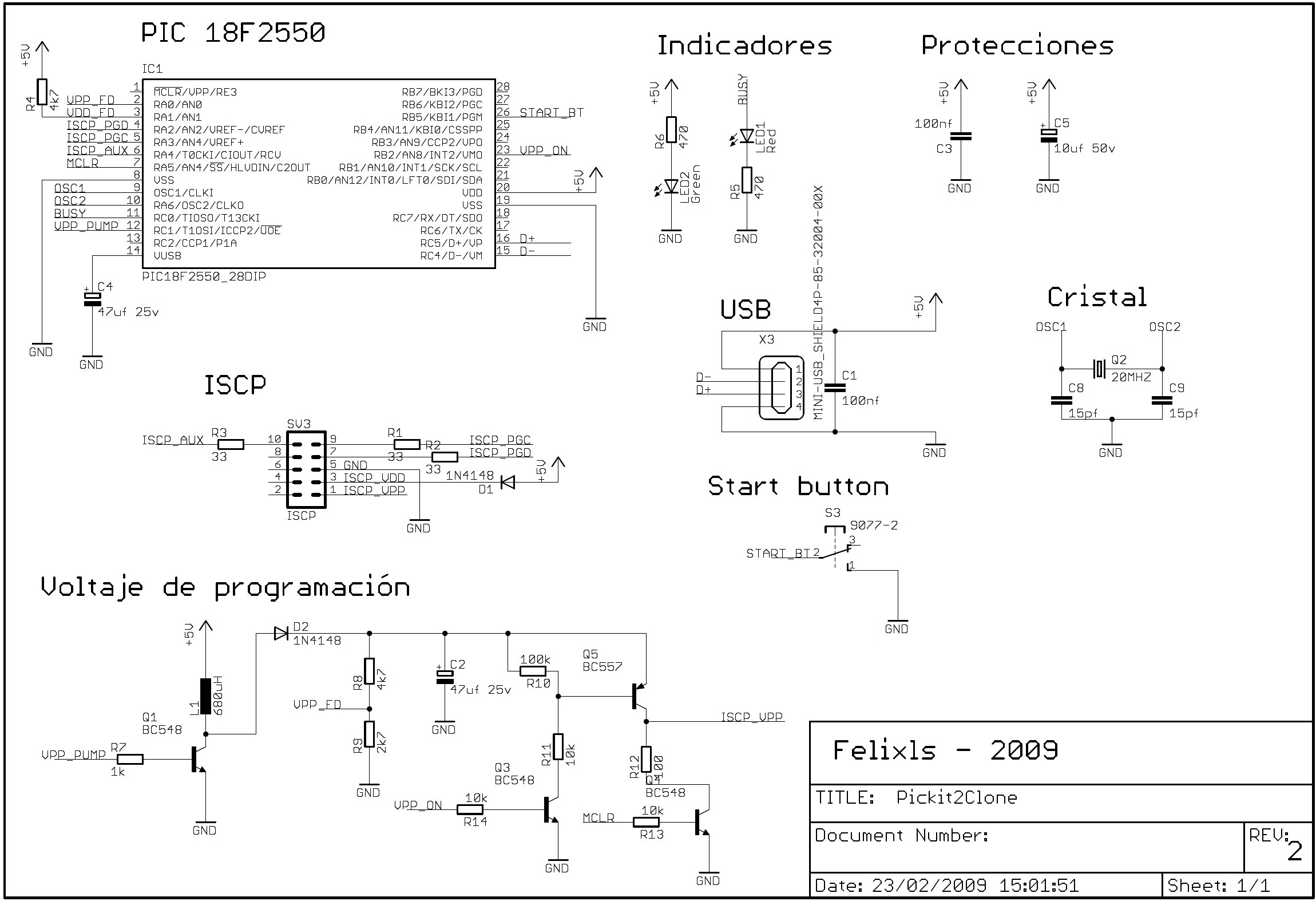
وهذا شرح عمل الدائره من هذا الموقع ..
http://proddec.org/?p=1935
Hai Friends here is a simple USB PIC Programmer. This is a modified version of Microchip’s PIC Kit 2. Documentations and other files of original PICkit2 are at the manufacturer’s site: Microchip PICkit2 site. By using this programmer, you can program all the 5v pic’s. 3.3v pic’s will require a small additional circuit. For programming we can use MPLAB or PIC Kit 2 ‘s software, which is available to download at the microchips site Programming is done through ICSP (In Circuit Serial Programming)
All the operations are accomplished by the PIC18F2550. It convers the USB data to ICSP. The crystal X1 is used to generate clock , the capacitors C2 and C3 stabilize the clock. At the time of programming PIC Micro controllers need 12v VPP, L1, Q1, D1, C1 and C4 form a boost DC – DC converter to boost 5v DC from USB port to 12v DC. A voltage sensing feedback is given to the analog input AN0 using R2 and R3. Q4 and Q5 with R5 are used for switching MCLR/VPP output during programming. Q6 with R4 gives an active pull-down to MCLR line when it is needed. LED1 (green, with R12) shows that the clone consumes power supply from the USB. R16 and Q3 are for switching the Vdd on the output Vdd line. Vdd sensing feedback to the PIC is worked up with R6. Q2 with R1 and R17 form the active pull-down at the output Vdd line. The D2 (if fitted) only protects the circuit against external voltage from Vdd. Yellow colored LED2 (with its series resistor R11) indicates that Vdd is switched to the output. The red LED3 (with R10) is controlled by the firmware to indicate different states of operating. Normally it lights during the read and write operations, means “busy” state. R7, R8 and R9 are current limiting resistors in series the output lines PGD, PGC and AUX. R15 and R14 ensures the low level at the PGD and PGC lines in certain cases. C5, C6 and C7 are power-line decoupling capacitors while R13 acts as a discharger load after disconnecting the device from USB. S1 push-button has two functions:
• holding down during connecting PICkit2 to the USB the device starts in a special bootloader mode – in this mode only downloading a new firmware is available from the PICkit2 handling software;
• during normal operation a push can trigger the handling software to reload the last used hex file and program it to the attached device if this is enabled in the software.
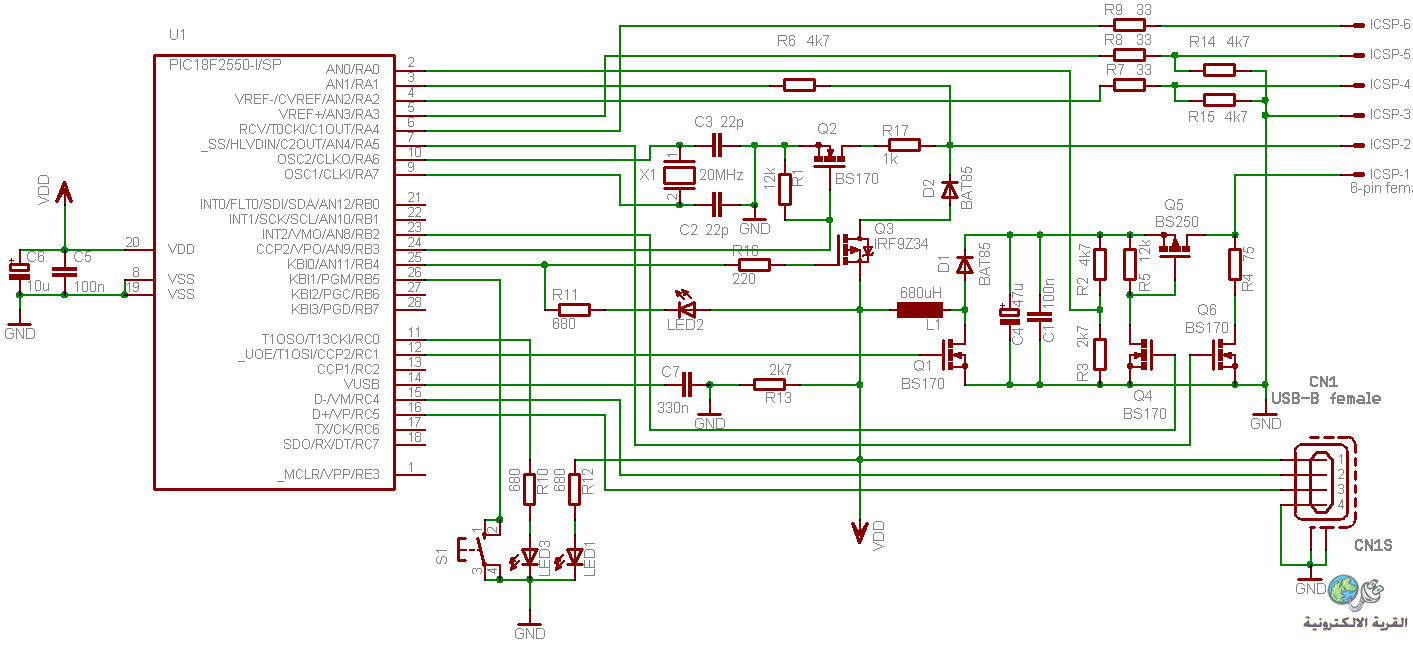
The PCB design and fitting picture can be downloaded from below. It is one-sided, only some straight wires can be found on the component side (red lines). This makes it easy to print the board at home too. I put a text onto the PCB to make easier to identify the right side of the layout. This is a crucial part that you have to be able to read the text on the copper – so you can double check it before the etching. Layout has been exported from Eagle into PNG format with 600 dpi resolution. A friend of mine had been converted the image to PDF, it looks fine too. The pictures with the original size and Eagle files can be found in the package of the article at our download area - click here to download! You must know that protection diode D2 (BAT85 on schematics) drops much more voltage on Vdd line than the switching FET Q3. If you wish, the voltage drop of the protection diode can be eliminated by shorting the place of it. If you don’t want to totally cancelling this protection, you can use a lower drop type, eg. 1N5819. The PIC is better to build in using a socket. Design around Q3 allows you to replace the Q3 (IRF9Z34) with a significantly cheaper BC640 bipolar transistor (as you can see on my prototype). In this case the output current is limited to a few hundred milliamperes with an acceptable voltage drop. Otherwise, assembling the board is not a complicated task, although bewaring of the accidental shorts is essential. After populating the PCB up you would check the electrical connections with a buzzer (continuity tester).
The first startup
Unfortunately to start the clone you have to program the firmware into the 18F2550 – you will need a secondary programmer for this. Once the PICKit2 firmware has been programmed into the 18F2550, you can upgrade it without the need of another programmer, because the firmware also includes a bootloader. After electrical checks against unwanted short- or open circuits on the PCB wires the board can be attached to a computer. Connecting the clone to the USB, the PC should detect it as a HID compliant device. In a Windows XP system open the device manager and check if it is there. Next, start the handling software “PICkit2″ and check the status reported by it. The status should show “PICkit2 connected.” text and shouldn’t be red backgrounded. If it seems to be all right, you should click on “troubleshoot” from “tools” menu and follow through the troubleshooting wizard. This procedure requires a voltage meter. Note, that the clone cannot regulate voltage on output Vdd line, so changing it in the PICkit2 program is irrelevant. You should always measure approximately the USB voltage (5V) on the Vdd output when it is turned on. Equivalent Substitutes For Unavailable Componets
• L1 inductor can vary between 470uH and 1mH, but it should be at least 150mA rated
• The power FET Q3 can effectively be replaced by a BC640 bipolar transistor sor IRF9540Ns
• BAT85s can be raplaced with BAT86, 1N5818 or 1N5819
• BS170 can be substituted by VN2010L or BS107
• BS250 can be substituted by VP2020L or BSS92 (be careful, BSS92 has different pinout!) sor BC 557 with base resistor s1K